
There is light our eyes will never see, a spectrum beyond red, where warmth itself speaks in photons too gentle to cross the visible threshold. The human eye stops listening there, but technology does not. Infrared vision allows us to perceive the heat of planets, the breath of clouds, and the slow glow of distant galaxies
Yet for semiconductors like Gallium Arsenide (GaAs), this world remains invisible. Infrared photons carry energies around 0.1 eV, far below GaAs’s bandgap of 1.43 eV, too weak to lift electrons from the valence to the conduction band. So if nature will not let us see, we must engineer a way to listen differently, not across the bandgap, but within it.
That is the idea behind the \(\textbf{Quantum Well Infrared Photodetector (QWIP)}\), a device that turns confinement into sensitivity, making electrons feel what they once ignored.
1. The Birth of a Well
At the heart of every QWIP lies a simple structure: alternating layers of \(\textbf{GaAs}\) and \(\textbf{Al$_x$Ga$_{1-x}$As}\), grown with atomic precision using \(\textbf{Molecular Beam Epitaxy (MBE)}\). The difference in their band gaps forms a periodic potential landscape, GaAs wells separated by AlGaAs barriers.
\( \begin{aligned} \text{Barrier: } & \text{Al}_{x}\text{Ga}_{1-x}\text{As}, \quad E_g \approx 1.9\,\text{eV} \\ \text{Well: } & \text{GaAs}, \quad E_g = 1.43\,\text{eV} \end{aligned} \)
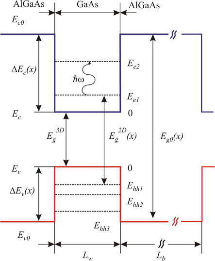
Within the well, an electron’s energy is no longer continuous; it becomes quantized:
\( E_n = \frac{h^2 \pi^2 n^2}{2 m^* L_w^2} \)
where \(m^*\) is the electron’s effective mass and \(L_w\) the well width.
These discrete states, \(E_1\), \(E_2\), \(E_3\), behave like steps on a ladder, equally spaced in potential but separated by forbidden zones. Quantum confinement transforms a smooth sea of energy into a finely tuned resonator.
The metaphor is almost poetic: restriction giving rise to precision. The narrower the well, the higher the note the electron can sing.
2. From Confinement to Detection
A QWIP does not rely on interband transitions (valence to conduction) like conventional photodiodes.
Instead, it listens for intersubband transitions, subtle jumps between energy levels inside the conduction band.
When an infrared photon of energy \(h\nu = E_2 – E_1\) strikes the device, it excites an electron from its ground state \(E_1\) to the excited state \(E_2\) within the same quantum well.
\( E_{\text{photon}} = h\nu = E_2 – E_1 \)
This process is possible because confinement breaks the continuous spectrum of motion into discrete levels, allowing photons of specific wavelengths to couple efficiently.
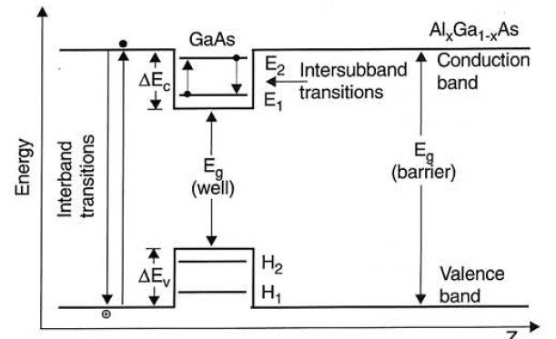
However, for a signal to appear, the electron must escape the well. An electric field applied across the device tilts the potential landscape, giving the excited electron a downhill path to drift toward the contact. This produces the photocurrent, the measurable signature of infrared detection.
In laboratory spectra, the response peaks sharply at the resonant transition energy. Adjusting the well width and aluminum content tunes this response, allowing detection across various infrared bands (typically 8–12 µm for thermal imaging, 3–5 µm for mid-IR sensing).
3. Engineering the Spectrum
Quantum engineering gives QWIPs a rare gift, tunability. By modifying structural parameters, the designer chooses which slice of the infrared spectrum the device “hears”:
| Design Parameter | Physical Effect | Outcome |
|---|---|---|
| Well width (\(L_w\)) ↓ | Subband spacing ↑ | Detects shorter wavelength |
| Al composition (\(x\)) ↑ | Barrier height ↑ | Improves confinement, lowers tunneling |
| Doping concentration ↑ | Increases carrier density | Raises dark current if excessive |
| Number of wells ↑ | Increases absorption | Enhances sensitivity |
Most practical devices use multi-quantum-well (MQW) stacks, often 40 to 60 wells, to amplify absorption while maintaining uniformity. Because each well absorbs only a small fraction of incoming light, repetition is key.
4. From The Lab to The Sky
The QWIP’s simplicity, uniformity, and compatibility with GaAs technology have made it a workhorse in modern infrared sensing. Research at NASA’s Jet Propulsion Laboratory (JPL) refined these detectors into high-performance imaging arrays.
Typical parameters:
- Peak response: 8–12 µm (Long-Wavelength IR, LWIR)
- Noise Equivalent Differential Temperature (NEDT): ≈30–36 mK
- Array sizes: 320×256 and 640×486 pixels
- Operating temperature: 60–70 K
Applications span from astronomy and earth observation satellites to thermal surveillance and defense imaging systems. QWIPs have captured volcanic heat plumes, planetary atmospheres, and the faint thermal glow of deep space.
5. The Challenge and the Elegance
QWIPs are not perfect. Because intersubband transitions are polarized along the growth direction, these detectors are sensitive only to the component of electric field perpendicular to the layers, requiring grating couplers or oblique incidence to couple normal radiation. They also require cryogenic cooling to suppress dark current.
Yet their elegance lies in reproducibility and design precision. Unlike more complex quantum dot or type-II superlattice detectors, QWIPs offer unmatched uniformity and manufacturability. Each electron behaves predictably, each layer grows with angstrom-scale consistency.
6. Beyond the Visible
In every quantum well, an electron waits in silence until the right photon arrives, a reminder that awareness often begins in stillness. The QWIP does not fight against the rules of physics; it uses them gently, confining electrons just enough to make them sensitive to the unseen.
By shaping limitation, it opens perception. By trapping energy, it reveals the invisible.
And in that delicate balance of confinement and revelation lies the quiet genius of the Quantum Well Infrared Photodetector.